


Related Posts

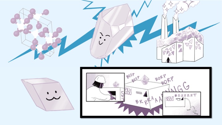
Students learn how some crystals produce electricity when squeezed! This lesson is part 4 of a 4-part student-driven, lecture-free series, in which students will do card sorts, build hands-on models, solve engineering design puzzles, and more!

Students make paper models of crystal unit cells and build a large crystal structure together while reflecting on the role of symmetry in crystal formation. This lesson is part 3 of a 4-part student-driven, lecture-free series, in which students will do card sorts, build hands-on models, solve engineering design puzzles, and more!
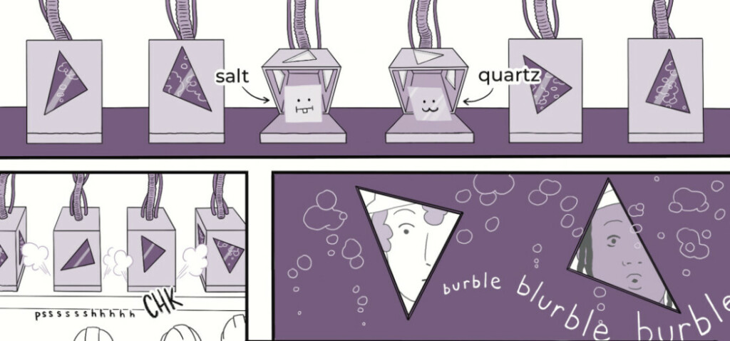
Crystals aren't magic, but they are amazing! In this engaging, comic-driven lesson, students do individual and group-based activities to understand the characteristics of crystals (like quartz) versus amorphous solids (like glass). This lesson is part 1 of a 4-part student-driven, lecture-free series in which students will do card sorts, build hands-on models, solve engineering design puzzles, and more!
More Funsize Research

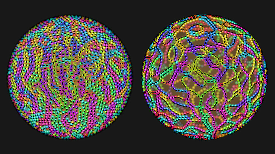
Scientists can use DNA to form nanoblocks of almost any shape and then assemble them into complex three-dimensional structures. Click to explore this fantastic new nanoworld!
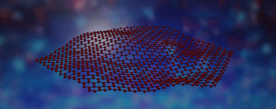
Welcome to the fascinating world of two-dimensional (2D) materials! Today, we're going to explore a novel 2D material created by boiling off atoms, which we guide to form large crystalline flakes that will become the filling in tiny magnetic sandwiches. Intrigued? Click to learn more!

You take a pristine-looking Oreo from a package of seemingly identical sandwich cookies, and you decide to open it up to eat the creme filling first. You gently twist the cookie apart without breaking the chocolate wafers, but the creme sticks to one side only. Why? Happily, the physics of fluids helped two MIT students solve this delicious mystery. Read on to find out what they learned, and how you can test their results at home.
The future of wearable electronics will be smart skins, e-textiles, and other flexible devices. To create these devices, we need new materials that can bend and stretch, but still conduct heat and electricity like traditional metals. Liquid metals to the rescue—read on to learn more!

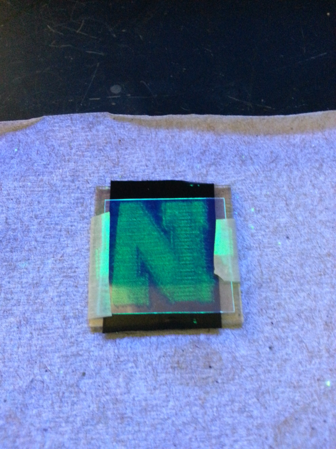
Instead of pencil, paper, and eraser, we can use combinations of lasers and magnetic materials to write, read, and and erase information by varying the temperature and magnetic field. Here we apply our laser "pencil" to magnetic "paper" to write the letter “N” (Go Huskers!!). This technique allows us write, erase, and rewrite tiny magnetic memories like those found in your computer hard drive and other devices. Click to learn how it works!
Measurements of the three-dimensional motion of fibers in turbulent fluid flow are helping us understand the multiphase flows involved in making paper.
It’s a hot summer day. You desperately want something cold to drink, but unfortunately, your bottle of root beer has been sitting in a hot car all day. You put it into a bucket full of ice to cool it down. But it’s taking forever! How, you wonder, could you speed the process up? The same question is important for understanding how electronic devices work, and how we can make them work better by controlling the temperature of the electrons that power them. Read on to find out what a bottle of root beer in a cooler full of ice and a nanowire in a vat of liquid helium have in common!
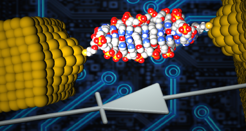
Diodes, also known as rectifiers, are a basic component of modern electronics. As we work to create smaller, more powerful and more energy-efficient electronic devices, reducing the size of diodes is a major objective. Recently, a research team from the University of Georgia developed the world's smallest diode using a single DNA molecule. This diode is so small that it cannot be seen by conventional microscopes.
You may have heard that there are three main phases of matter: solids, liquids, and gases (plus plasma if you want to get fancy). Liquids can take virtually any shape and deform instantly. Solid materials possess interesting electronic and magnetic properties essential to our daily life. But how about designing rigid liquids with magnetic properties? Impossible? Not anymore. Click to learn more!

We think we're pretty familiar with how ordinary liquids behave, but it turns out that some of the basic things we know are no longer true when we look at these liquids on short enough length scales and fast enough time scales. The liquids start to behave more like solids, pushing back when you push on them, and slipping across solid surfaces instead of being dragged along. Click to ride the tiny-but-mighty new wave of nanofluidics!
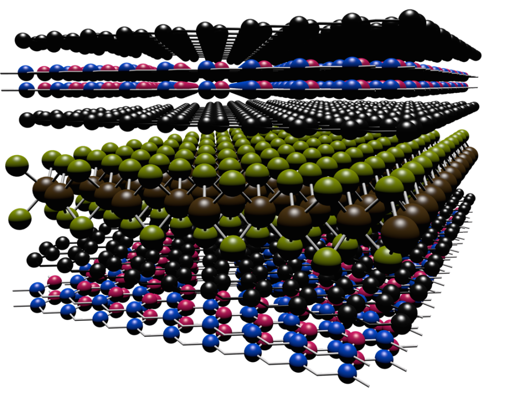
Scientists have developed a way to engineer new forms of matter by stacking different types of layers, each only one atom thick, on top of one another.
Scientists are working to develop electronic devices that store and process information by manipulating a property of electrons called spin—a research area aptly known as spintronics. The semiconductors we are developing will not only be faster and cheaper than those used in conventional devices, but will also have more functionality.
Materials that are absolutely perfect—in other words, materials that contain no defect of any kind—are usually not very interesting. Imagine being married to a saint: you would quickly be bored out of your mind! Defects and impurities can considerably change many properties of materials in ways that allow a wide range of applications.

Semiconductors are materials with properties intermediate between metals and non-conducting insulators, defined by the amount of energy needed to make an electron conductive in the material. The non-conducting electrons occupy a continuum of energy states, but two of these states (the “heavy hole” and “light hole”) are nearly identical in energy. The heavy hole is easy to observe and study, but the light hole eludes most observers.
Solids are generally divided into metals, which conduct electricity, and insulators, which do not. Some oxides straddle this boundary, however: a material's structure and properties suggest it should be a metal, but it sometimes behaves as an insulator. Researchers at the University of California, Santa Barbara are digging into the mechanisms of this transformation and are aiming to harness it for use in novel electronic devices.
You may know that the media used in magnetic recording technologies, such as computer hard drives, are made of millions of tiny nanomagnets. Each nanomagnet can be switched up or down to record bits of information as ones and zeros. These media are constantly subjected to magnetic fields in order to write, read, and erase information. If you have ever placed a magnet too close to your laptop or cell phone, you know that exposure to an external magnetic field can disrupt information stored this way. Did you know that it is possible for the nanomagnets to "remember" their previous state, if carefully manipulated under specific magnetic field and temperature conditions? Using a kind of memory called topological magnetic memory, scientists have found out how to imprint memory into magnetic thin films by cooling the material under the right conditions.
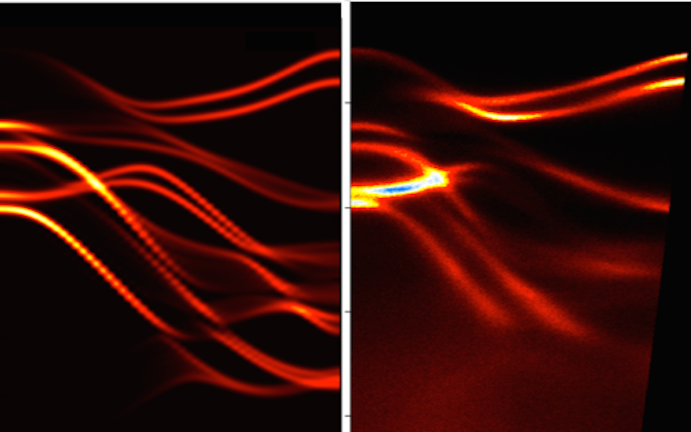
Inside solids, the properties of photons can be altered in ways that create a kind of "artificial gravity" that affects light. Researchers at the University of Pittsburgh tracked photons with a streak camera and found that whey they enter a solid-state structure, they act just like a ball being thrown in the air: they slow down as they move up, come to a momentary stop, and fall back the other way. Studying this "slow reflection" will allow us to manipulate light's behavior, including its speed and direction, with potential applications in telecommunications and quantum computing technologies.
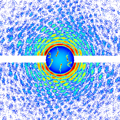
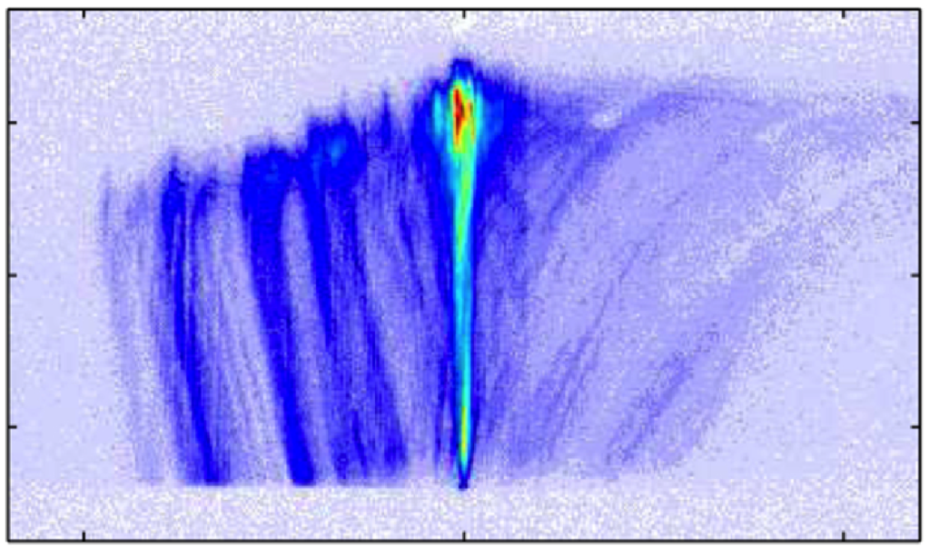
In a unique state of matter called a superfluid, tiny "tornadoes" form that may play an important role in nanotechnology, superconductivity, and other applications. Just as tornadoes are invisible air currents that become visible when they suck debris into their cores, the quantum vortices in superfluids attract atoms that make the vortices visible. Quantum vortices are so small they can only be imaged using very short-wavelength x-rays, however.
Would you rather have data storage that is compact or reliable? Both, of course! Digital electronic devices like hard drives rely on magnetic memory to store data, encoding information as “0”s and “1”s that correspond to the direction of the magnetic moment, or spin, of atoms in individual bits of material. For magnetic memory to work, the magnetization should not change until the data is erased or rewritten. Unfortunately, some magnetic materials that are promising for high density storage have low data stability, which can be improved by squeezing or stretching the crystal structures of magnetic memory materials, enhancing a material property called magnetic anisotropy.
Neutron radiation detection is an important issue for the space program, satellite communications, and national defense. But since neutrons have no electric charge, they can pass through many kinds of solid objects without stopping. This makes it difficult to build devices to detect them, so we need special materials that can absorb neutrons and leave a measurable signature when they do. Researchers at the University of Nebraska-Lincoln are studying the effects of solar neutron radiation on two types of materials on the International Space Station (ISS), using detectors made of very stable compounds that contain boron-10 and lithium-6.

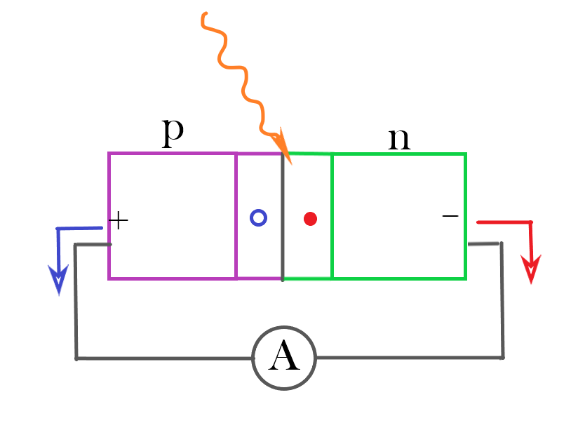
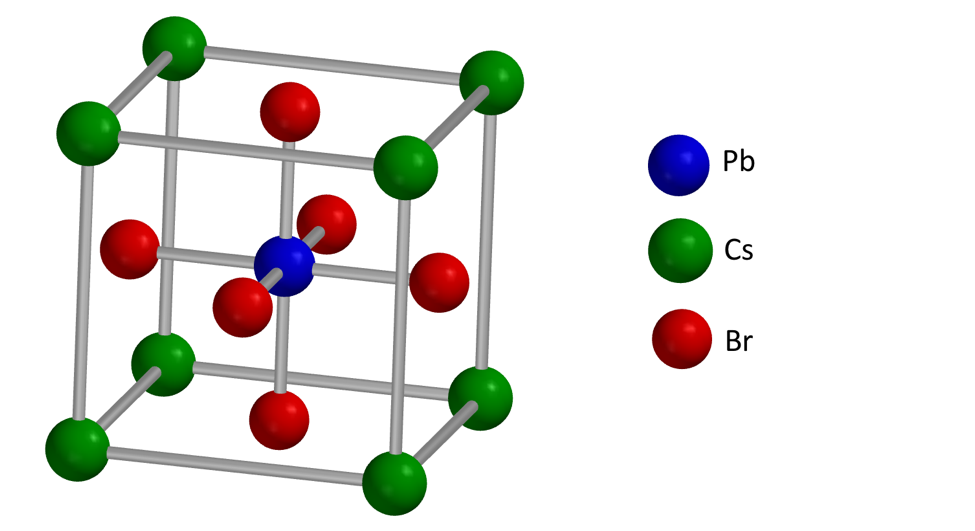
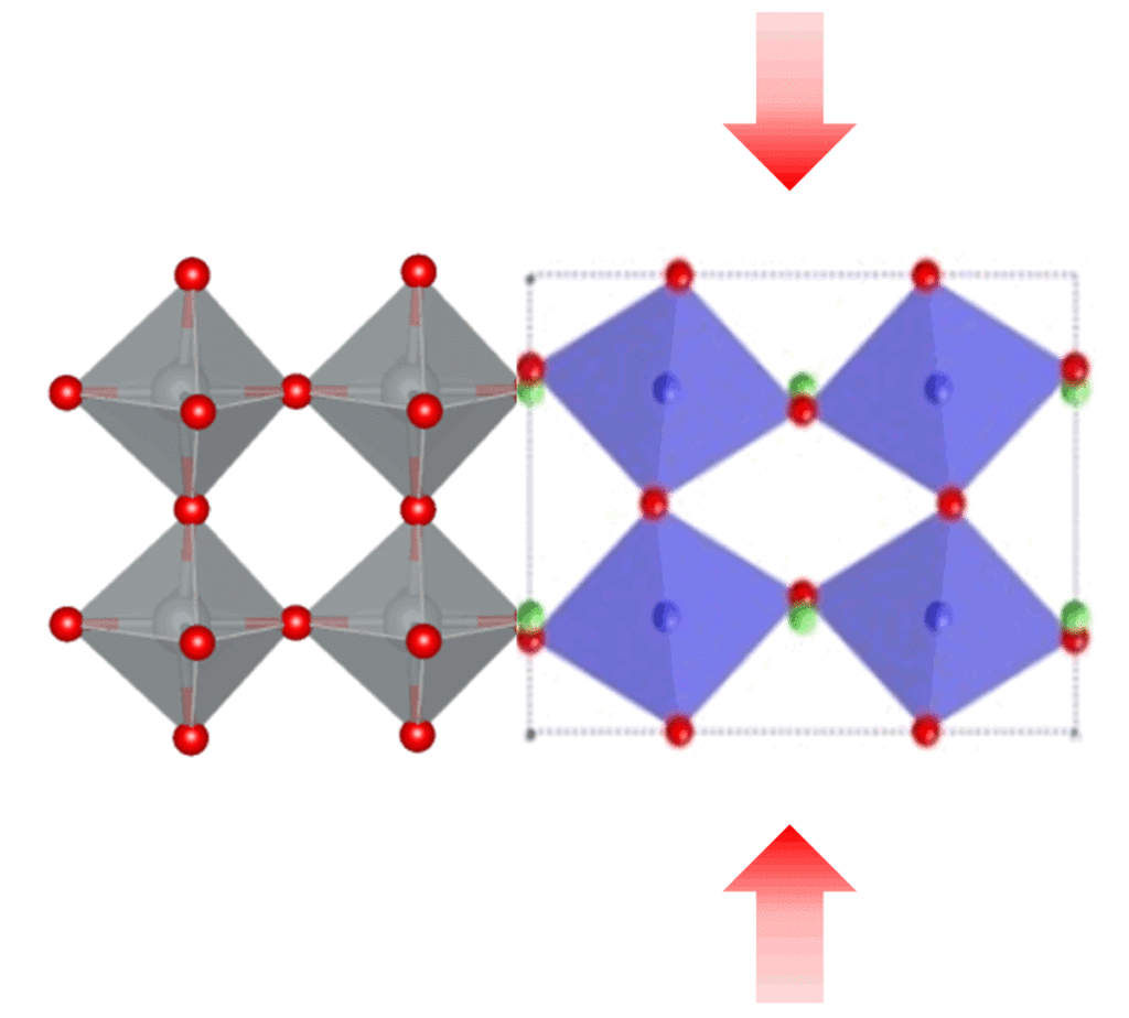
To increase our use of solar energy, we need to create more efficient, stable, and cost-effective solar cells. What if we could use an inkjet printer to fabricate them? A new type of solar cell uses a class of materials called perovskites, which have a special crystal structure that interacts with light in a way that produces an electric voltage. We've developed a method to produce perovskite thin films using an inket printer, which in the future could pave the way to manufacture solar cells that are surprisingly simple and cheap.